Scientists Built a Particle Accelerator Smaller Than a Human Hair on a Chip
Credit to Author: Becky Ferreira| Date: Thu, 02 Jan 2020 19:44:56 +0000
The world’s biggest particle accelerator, the Large Hadron Collider, is a gargantuan structure that extends underground for 17 miles and cost several billion dollars to build and operate.
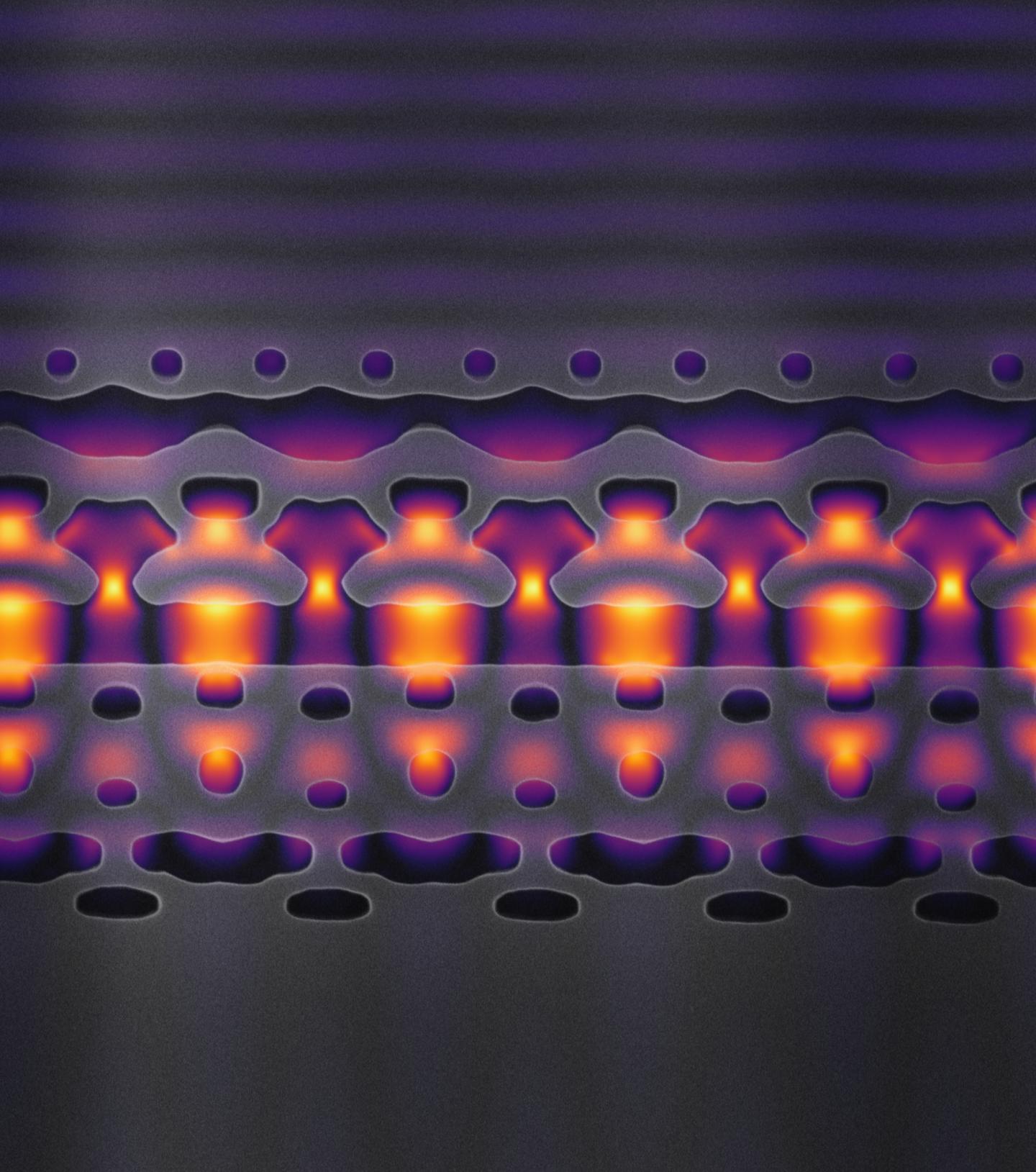
Now, scientists have developed a particle accelerator on the other end of the size spectrum, measuring just 30 microns across—about half the width of a human hair—according to a study published on Thursday in Science.
The tiny instrument is the latest breakthrough in an international effort to develop an “accelerator-on-a-chip,” a class of miniaturized particle accelerators with a wide range of potential applications in materials science, chemistry, and medicine.
The microscale machine, which is called a dielectric laser accelerator (DLA), could eventually lead to a cheaper and more compact version of accelerators that operate in the megaelectronvolt (MeV) energy range. These instruments include X-ray machines, radiation devices for cancer treatments, and industrial scanning equipment, among many others.
“The idea is to shrink those types of particle accelerators down—the ones that operate on the MeV scale,” said lead author Neil Sapra, a graduate student at Stanford University, in a call. “A MeV scale and a low current is where the DLA shines.”
“If you look at the design, no human engineer would have come up with it”
Previous experiments have demonstrated that a light source called a free-space laser can accelerate particles within microscale structures. The new prototype developed by Sapra’s team improves on that research with a new design that could be gradually scaled up to a MeV capacity, and could accelerate particles to about 94 percent the speed of light.
“What’s important about this work is that it’s the first on-chip demonstration of a dielectric laser accelerator,” Sapra said. “So, this is a pathway to scalability and to greater robustness.”
The researchers were able to achieve this breakthrough with a technique called a “photonic inverse-design approach,” which means that the accelerator’s design was generated by a computer that used optimization algorithms to account for light’s finicky behavior in nanoscale structures.

The structure that satisfied the team’s parameters is a chip covered in mesa-like plateaus that are engraved with channels to corral electrons. When blasted with an infrared laser pulse, the electrons receive a speed boost and an energy level of about 1 kiloelectronvolt (KeV).
“If you look at the design, no human engineer would have come up with it,” Sapra explained. “I really don’t think I could have done this project without this inverse-design technique because coming up with a design is pretty difficult doing the classical approach.”
At this point, the new DLA design can only administer one jolt of acceleration to the electrons, and it will need to scale up to about 1,000 jolts to get into the MeV range. Sapra’s team thinks it will take about five to 10 years to build that prototype, which could reduce cost and increase precision for multiple fields, especially healthcare.
“These integrated photonic circuits are based on the same methods that the electronics industry is built off of, so it’s not just making something smaller, it’s making something cheaper,” Sapra said.
This article originally appeared on VICE US.